PCF8591 ADC/DAC (AD/DA) Analog Digital Conversion Module
This PCF8591 Integrated Circuit Module is recommended for use with micro controllers or development boards that have a limited number of ADC ports or do not meet the required specifications. Also, the conversion function from digital to analogue is also very useful.
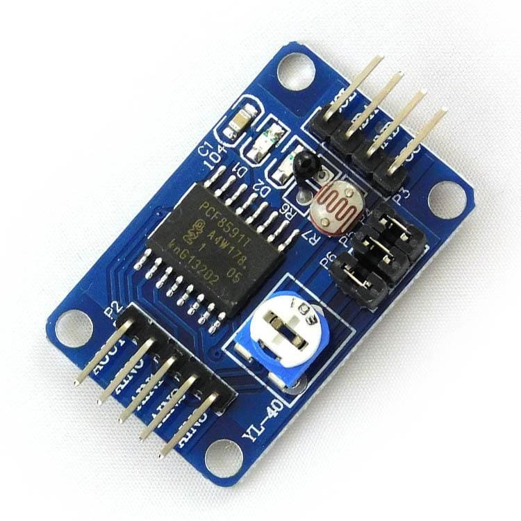
This product already contains a light sensor with photo resistor, a thermistor, and a potentiometer that can provide analog values.
This module is useful for processing data from analog sensors such as distance, temperature, humidity, and so on.
Description:
The PCF8591 is a monolithically integrated, and a separate power supply, low-power, 8-bit CMOS data acquisition devices. The PCF8591 has the four analog inputs, one analog output and a serial I2C bus interface.
PCF8591 three address pins A0, A1 and A2 can be used in hardware address programmed 8 PCF8591 device allows access to the same I2C bus, without the need for additional hardware. On the PCF8591 device input and output of the address, control and data signals are transmitted in serial fashion via the two-wire bidirectional I2C bus.
PCF8591 IC Features:
- Single power supply
- PCF8591 operating voltage range of 2.5V-6V
- Low standby current
- Via I2C bus serial input / output
- PCF8591 by 3 hardware address pins addressing
- PCF8591 I2C bus speed sampling rate decided
- 4 analog inputs programmable single-ended or differential input
- Automatic incremental channel selection
- PCF8591 analog voltage range from VSS to VDD
- PCF8591 built-in track-and-hold circuit
- 8-bit successive approximation A / D converter
- 1 analog output DAC gain
Module Features:
- Module chip using PCF8951
- Module supports external voltage input of the 4-way acquisition (voltage input range of 0-5v)
- The module integrated photoresistor by AD collection precise value of the ambient light intensity
- Module integrated thermistor by the precise value of the ambient temperature of the AD acquisition
- Module integrated 1 channel 0-5V voltage input acquisition (the blue potentiometer to adjust the input voltage)
- Modules with power indicator (for the module power supply indicator lights)
- Modules with DA output indicator, when the module DA output interface voltage reaches a certain value, will be lit panel the DA output indicator, the higher the voltage, the more obvious indicator brightness
- Module PCB size: 3.6cm * 2.3cm
- Standard double panel, thickness 1.6mm, nice layout, surrounded by a through-hole, aperture: 3mm, convenient fixed
Module interface specification:
The Left
- AOUT chip DA output interface
- AINO chip analog input interface 0
- AIN1 chip analog input interface 1
- AIN2 chip analog input interface 2
- AIN3 chip analog input interface 3
The Right
- SCL – IIC clock interface connected to microcontroller IO port
- SDA – IIC digital interface connected to microcontroller IO port
- GND – connected to ground
- VCC – connected to 3.3v-5v
- Four red jumper-cap instruction
- P4 – connected to P4 shorting cap, select thermistor access circuit
- P5 – connect P5 shorting cap, select photo-resistor access circuit
- P6 – connected to P6 shorting cap, select 0-5V adjustable voltage access circuit
You must be logged in to post a review.
Related products
(OV5647) Raspberry Pi Night Vision Camera Module
ARDUINO A000073 (UNO SMD REV3, ATmega328 MCU)
Arduino Ethernet Shield w/o PoE (Wiznet W5100)
(Get A latest Price)
Atmega32u4 Esplora Joystick Game Programming Module
Overview:
Microcontroller: ATmega32u4 Operating Voltage: 5V Flash Memory: 32 KB of which 4 KB used by bootloader SRAM: 2.5 KB EEPROM: 1 KB Clock Speed: 16 MHz The board contains everything needed to support the microcontroller; simply connect it to a computer with a USB cable to get started. The Esplora has built-in USB communication; it can appear to a connected computer as a mouse or keyboard, in addition to a virtual (CDC) serial / COM port. This has other implications for the behavior of the board. Arduino DIY Experiment is mainly used for kids toys,science kits for 10 year old kids, steam kit on high school, primary school, secondary school, cool science experiments.Leonardo R3 Development Board ATMEGA32U4
Product specifications:
• Controller: ATmega32u4 • Work record: 16 MHz • Working voltage: 5V • Input voltage (recommended): 7-12V • Digital IO port: 20 • PWM channel: 7 • Analog input: 12 • 5V digital / analog port maximum allowable current: 40 mA • 3.3V digital / analog port maximum allowable current: 50 mA • Flash Memory: 32 KB (ATmega32u4) of which 4 KB used by bootloader • SRAM: 2.5 KB (ATmega32u4) • EEPROM: 1 KB (ATmega32u4)Mega+WiFi R3 ATmega2560+ESP8266 32Mb Flash Memory USB-TTL CH340G Micro USB port
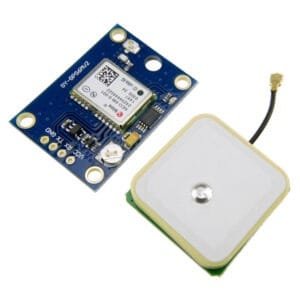
U-BLOX NEO-6M module (GY-GPS6MV2)
- 1 — u-blox NEO-6M GY-GPS6MV2 GPS module with on board EEPROM
- 1 — GPS antenna
- 1 — 1x4 male header
WiFly RN-171
- Ultra low power for battery powered applications
- Firmware configurable transmit power: 0dBm to +12dBm
- Hardware interfaces: UART
- Supports Adhoc and infrastructure networking modes
- User programmable GPIO & ADCs
- Real-time clock for time-stamping, auto-sleep, and auto-wakeup modes
- Run directly from batteries or regulated power supplies
- Configuration over serial or wireless interface using simple ASCII commands
- Over the air firmware upgrade
- Secure Wi-Fi authentication schemes (WEP/WPA/WPA2)
- Full onboard TCP/IP stack (no external drivers required)








Reviews
There are no reviews yet.